What Are the Different Types of HDI Structures?
Different Types of HDI Structures
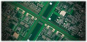
HDI (High-Density Interconnection) printed circuit boards use high-density copper layers to increase the number of connections within a small footprint. This allows for more components to be placed on the board, while preserving the integrity of the signal path. Typically, these boards have either a 2-layer or 4-layer core and include both plated through holes (PTH) and blind/buried vias.
This technology is often found in mobile cellular phones, touch-screen devices and portable video recording devices. It is also used in laptop computers, digital cameras and 4/5G network communications equipment, as well as military applications such as avionics and smart munitions.
PCBs made with hdi circuit board technology are lighter and smaller than conventional circuit boards due to their thinner inner and outer layers. They can also support higher frequencies and more complex designs than conventional technology, making them suitable for many electronic applications. The lower weight and compact size of HDI PCBs make them more cost-effective than traditional PCBs.
What Are the Different Types of HDI Structures?
The most important factor when designing an HDI PCB is selecting the right construction and stack-up for the application. The choice of materials has a major impact on the electrical performance of the traces and pads. The material must be able to withstand high temperatures and provide good signal transmission. It must also be able to accommodate the different electrical impedances required by digital, analog and power signals.
Another factor is the selection of the correct number of layers and types of interconnections, as this will directly influence manufacturing costs. It is recommended to stick with the minimum number of sequential layers required for the design, while considering the impact on the layer count on the routing capabilities of the board. Finally, it is essential to take into account the layout and placement of the various components and the spacing between them. It is critical to choose the proper components and place them in a way that will ensure a high level of installability, solderability and maintainability.
To increase the density of an HDI PCB, it is necessary to utilize microvias. These are small holes, typically less than 150 microns in diameter, that connect one layer of the PCB to the next. They are created using a laser drill and can be staggered or stacked. In addition, they can be filled with copper to improve signal transmission and allow for easier routing.
When designing an HDI PCB, it is important to keep in mind that it can be difficult to route through these small spaces. It is therefore essential to plan the component layout carefully and use a routing test to verify that all the features will work in the final product. It is also important to pay attention to the spacing between traces and pads. This will ensure that they are not too close together and cause crosstalk. Also, it is crucial to select the right layer for the placement of the ICs and avoid using unnecessary staggered or Extra-Large Inner Connects (ELIC) if possible.